Using Ports for I/O Operation
8051 is TTL logic device. TTL logic has two levels: Logic "High" (1) and logic "Low" (0). The voltage and current involved for the two levels are as follows:
Level | Voltage | Current |
High | Above 2.4V | Virtually no current flow |
Low | Below 0.9V | 1.6mA Sinking current from TTL input to ground (Depends on logic family) |
Ports | Function |
Port 0 (Pin 32-39) | Dual-purpose port- 1. general purpose I/O Port. 2. multiplexed address & data bus Open drain outputs |
Port 1 (Pin 1-8) | Dedicated I/O port – Used solely for interfacing to external devices Internal pull-ups |
Port 2 (Pin 21-28) | Dual-purpose port- 1. general purpose I/O port. 2. a multiplexed address & data bus. Internal pull-ups |
Port 3 (Pin 10-17) | Dual-purpose port- 1. general purpose I/O port. 2. pins have alternate purpose related to special features of the 8051 Internal pull-ups |
Port functions
The 8051 internal ports are partly bi-directional (Quasi-bi-directional). The following is the internal circuitry for the 8051 port pins:
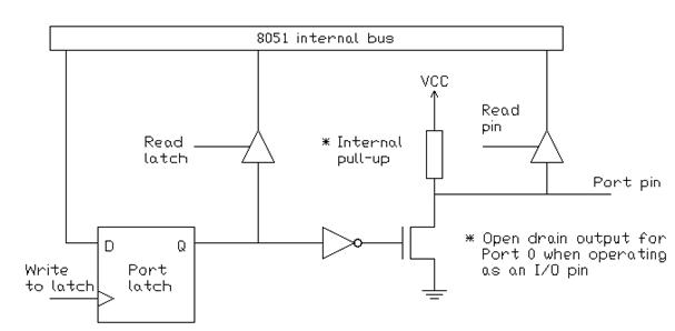
1.Configuring for output
P0 is open drain.
– Has to be pulled high by external 10K resistors.
– Not needed if P0 is used for address lines
Writing to a port pin loads data into a port latch that drives a FET connected to the port pin.
P0: Note that the pull-up is absent on Port 0 except when functioning as the external address/data bus. When a "0" is written to a bit in port 0, the pin is pulled low. But when a "1" is written to it, it is in high impedance (disconnected) state. So when using port 0 for output, an external pull-up resistor is needed, depending on the input characteristics of the device driven by the port pin
P1, P2, P3 have internal pull-ups: When a "0" is written to a bit in these port , the pin is pulled low ( FET-ON) ,also when 1 is written to a bit in these port pin becomes high (FET-OFF) thus using port P1,P2,P3 is simple.
2. Configuring for input
At power-on all are output ports by default
To configure any port for input, write all 1’s (0xFF) to the port
Latch bit=1, FET=OFF, Read Pin asserted by read instruction
You can used a port for output any time. But for input, the FET must be off. Otherwise, you will be reading your own latch rather than the signal coming from the outside. Therefore, a "1" should be written to the pin if you want to use it as input, especially when you have used it for output before. If you don't do this input high voltage will get grounded through FET so you will read pin as low and not as high. An external device cannot easily drive it high
so, you should not tide a port high directly without any resistor. Otherwise, the FET would burn.
Be Careful :
Some port pins serve multiple functions. Be careful writing to such ports. For example, P3.0 is the UART RXD (serial input), and P3.1 is the UART TXD (serial output). If you set P3.0 to a '0', an external buffer (such as an RS232 level translator) cannot drive it high. Therefore you have prevented receiving any serial input.
If an external interrupt such as EX1 on P3.3 is enabled, and set to be level sensitive, and you clear this pin's output latch to a zero, guess what? You've just caused a perpetual interrupt 1. The pin's input buffer will read the output of it's latch as always low. Your controller will spend all of its time in the interrupt handler code and will appear to have crashed, since it will have very little time for other tasks. In fact, it will get to execute a single instruction before re-entering the interrupt handler, so the rest of your program will execute very, very slowly.
SWITCH ON I/O PORTS

Good Circuit
It is always best connecting the switch to ground with a pull-up resistor as shown in the "Good" circuit. When the switch is open, the 10k resistor supplies very small current needed for logic 1. When it is closed, the port pin is short to ground. The voltage is 0V and all the sinking current requirement is met, so it is logic 0. The 10k resistor will pass 0.5 mA (5 Volt/10k ohm). Thus the circuits waste very little current in either state. The drawback is that the closure of switch gives logic 0 and people like to think of a switch closure gives logic 1. But this is not a matter because it is easy to handle in software.
Fair circuit
The "Fair" circuit requires that the pull-down resistor be very small. Otherwise, the pin will rise above 0.9V when the resistor passes the 1.6mA sinking current. When the switch is closed, the circuit waste a large current since virtually no current flows into the pin. The only advantage is that a switch closure gives logic 1.
Poor circuit
In the "Poor" circuit, the logic 1 is stable when the switch is closed. But when the switch is open, the input floats to a noise-sensitive high rather than a low. An open TTL pin is usually read as logic 1 but the pin may picks up noise like an antenna.
To conclude, driving a TTL input should always consider current sinking (pulling input to 0V).
LED ON I/O PORTS

Since TTL outputs is designed to feed multiple TTL inputs, they are good at current sinking but poor at current sourcing. The Standard TTL can sink up to 16mA and source 250uA. The LS logic family can sink 8mA and source 100uA. The 8051 port pin can sink 1.6mA (3.2mA for port 0) and source 60uA. Therefore, if you drive significant current, try to arrange your circuits to use current sinking.
Unlike diodes, Light-emitting diodes have a forward voltage drop from 1.7 to 2.5 volts and most of them flow a forward current 20mA.
Poor circuit
since the TTL output can't source above 1mA so the LED will be very dim.
Fair circuit
The LED will conduct heavily at about 2V and the extra 3V has to be dropped in the TTL circuitry. This causes high power dissipation in the TTL or the LED fails.
Good circuit
The resistor limits the current. The resistance can be calculated by assuming its voltage is about 2.5V and the TTL output is 0.9V. For 2.2V LED, 1.9V is across the resistor so the 220ohm would limit the current to 8.6mA (1.9/220). For 1.7V LED, 2.4V is across the resistor so it would limit the current to 10.9mA (2.4/220). The resistor should not less than 100ohm or the LED would fail.
8 LED’S EXAMPLE:

Connection -Port 1 is connected to eight LEDs, each of them is connected to 5V through a 330ohm resistor. Port 0 is connected to a DIP switch and a 10Kohm resistor
Condition - Corresponding led should light up when switch pressed , i.e. if Switch at 1.0 is pressed -> LED at P0.0 should light up.
CODE: